- 您现在的位置:买卖IC网 > Sheet目录369 > W9751G6IB-25 (Winbond Electronics)IC DDR2-800 SDRAM 512MB 84-WBGA
W9751G6IB
Notes:
1. To guarantee ODT off, V REF must be valid and a LOW level must be applied to the ODT pin.
2. V REF must be within ± 300 mV with respect to V DDQ /2 during supply ramp time.
3. V DD /V DDL voltage ramp time must be no greater than 200 mS from when V DD ramps from 300 mV to V DD min.
4. The V DDQ voltage ramp time from when V DD min is achieved on V DD to when V DDQ min is achieved on V DDQ must be no
greater than 500 mS.
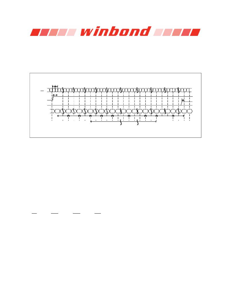
t CH t CL
CLK
CLK
CKE
ODT
t IS
t IS
Command
NOP
400nS
PRE
ALL
t RP
EMRS
t MRD
MRS
t MRD
PRE
ALL
t RP
REF
t RFC
REF
t RFC
MRS
t MRD
EMRS
Follow OCD
EMRS
t OIT
ANY
CMD
DLL
Enable
DLL
Reset
min 200 Cycle
OCD
Default
Flow chart
OCD
CAL. Mode
Exit
Figure 1 — Initialization sequence after power-up
7.2
Mode Register and Extended Mode Registers Operation
For application flexibility, burst length, burst type, CAS Latency, DLL reset function, write recovery
time (WR) are user defined variables and must be programmed with a Mode Register Set (MRS)
command. Additionally, DLL disable function, driver impedance, additive CAS Latency, ODT (On Die
Termination), single-ended strobe and OCD (off chip driver impedance adjustment) are also user
defined variables and must be programmed with an Extended Mode Register Set (EMRS) command.
Contents of the Mode Register (MR) or Extended Mode Registers EMR (1), EMR (2) and EMR (3) can
be altered by re-executing the MRS or EMRS Commands. Even if the user chooses to modify only a
subset of the MR or EMR (1), EMR (2) and EMR (3) variables, all variables within the addressed
register must be redefined when the MRS or EMRS commands are issued.
MRS, EMRS and Reset DLL do not affect array contents, which mean re-initialization including those
can be executed at any time after power-up without affecting array contents.
7.2.1
Mode Register Set Command (MRS)
( CS = "L", RAS = "L", CAS = "L", WE = "L", BA0 = "L", BA1 = "L", A0 to A12 = Register Data)
The mode register stores the data for controlling the various operating modes of DDR2 SDRAM. It
programs CAS Latency, burst length, burst sequence, test mode, DLL reset, Write Recovery (WR) and
various vendor specific options to make DDR2 SDRAM useful for various applications. The default
value in the Mode Register after power-up is not defined, therefore the Mode Register must be
programmed during initialization for proper operation.
The DDR2 SDRAM should be in all bank precharge state with CKE already HIGH prior to writing into
the mode register. The mode register set command cycle time (t MRD ) is required to complete the write
operation to the mode register. The mode register contents can be changed using the same command
and clock cycle requirements during normal operation as long as all banks are in the precharge state.
The mode register is divided into various fields depending on functionality. Burst length is defined by
A[2:0] with options of 4 and 8 bit burst lengths. The burst length decodes are compatible with DDR
Publication Release Date: Oct. 23, 2009
- 10 -
Revision A06
发布紧急采购,3分钟左右您将得到回复。
相关PDF资料
W9751G6KB-25
IC DDR2 SDRAM 512MBIT 84WBGA
W9812G6JH-6I
IC SDRAM 128MBIT 54TSOPII
W9816G6IH-6I
IC SDRAM 16MBIT 50TSOPII
W9825G6JH-6I
IC SDRAM 256MBIT 54TSOPII
W9864G6JH-6I
IC SDRAM 64MBIT 54TSOPII
WM-5614
CABINET WALL MOUNT 37.25X17.9"
WRR-2244
RACK WALL MOUNT RELAY 42" X 19"
WRR-2264
RACK WALL MOUNT 75.25" X 19"
相关代理商/技术参数
W9751G6JB
制造商:WINBOND 制造商全称:Winbond 功能描述:8M ? 4 BANKS ? 16 BIT DDR2 SDRAM
W9751G6JB-25
制造商:Winbond Electronics Corp 功能描述:512GB DDRII
W9751G6JB-3
制造商:Winbond Electronics Corp 功能描述:512MB DDRII
W9751G6KB
制造商:WINBOND 制造商全称:Winbond 功能描述:8M ? 4 BANKS ? 16 BIT DDR2 SDRAM
W9751G6KB-18
制造商:Winbond Electronics Corp 功能描述:IC MEMORY
W9751G6KB-25
功能描述:IC DDR2 SDRAM 512MBIT 84WBGA RoHS:是 类别:集成电路 (IC) >> 存储器 系列:- 标准包装:1 系列:- 格式 - 存储器:闪存 存储器类型:闪存 - NAND 存储容量:4G(256M x 16) 速度:- 接口:并联 电源电压:2.7 V ~ 3.6 V 工作温度:0°C ~ 70°C 封装/外壳:48-TFSOP(0.724",18.40mm 宽) 供应商设备封装:48-TSOP I 包装:Digi-Reel® 其它名称:557-1461-6
W9751G6KB25A
制造商:WINBOND 制造商全称:Winbond 功能描述:Double Data Rate architecture: two data transfers per clock cycle
W9751G6KB25I
制造商:Winbond Electronics Corp 功能描述:DRAM Chip DDR2 SDRAM 512M-Bit 32Mx16 1.8V 84-Pin WBGA 制造商:Winbond Electronics Corp 功能描述:IC DDR2 SDRAM 512MBIT 2.5NS BGA
